Recently, metamaterials have drawn a great deal of attention in the research community. Due to their exotic electromagnetic properties resulted from the artificially tailored electric and magnetic responses; metamaterials have been used to create negative refraction, subwavelength image resolution, and cloaking effects. In most cases, efforts have been made to reduce electric and magnetic loss of metamaterials. Actually, the loss of metamaterials can also be used as electromagnetic wave attenuations. The objective of this project is to design ultra-thin absorbers with metamaterials.
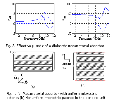
An ultra-thin (t ≈ λ/50) microstrip metamaterial absorber is illustrated in Fig. 1. It consists of three parts: periodic metal patches, lossy dielectric or magnetic substrate with thickness of t, and a backing metal wall. Due to strong magnetic resonance of the structure, strong artificial magnetism can occur (Fig. 2).
The effective µ and ε can be tuned by changing either the patch size or the electromagnetic properties of the substrate. Thus, the absorption bandwidth of the metamaterial absorber could be broader than common absorbers (Fig. 3).
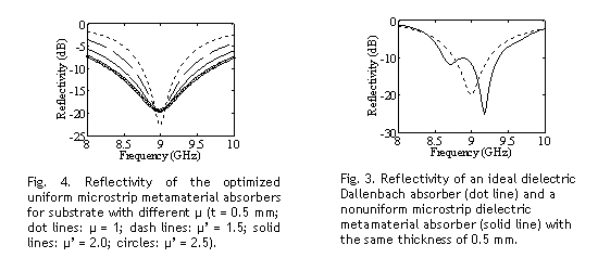
By using proper substrate and metal patches, the bandwidth of the metamaterial absorber can be increased when using substrate with larger µ (Fig. 4). The ultimate bandwidth limit of the metamaterial absorbers is expressed as follows:

Where c is the speed of light in free space, f0 is the center frequency in the waveband Δf, and  . ρ0 is the given absorption level. It is obvious that, with the increase of the static permeability (µs) and the thickness of the substrate, the bandwidth limit increases.